

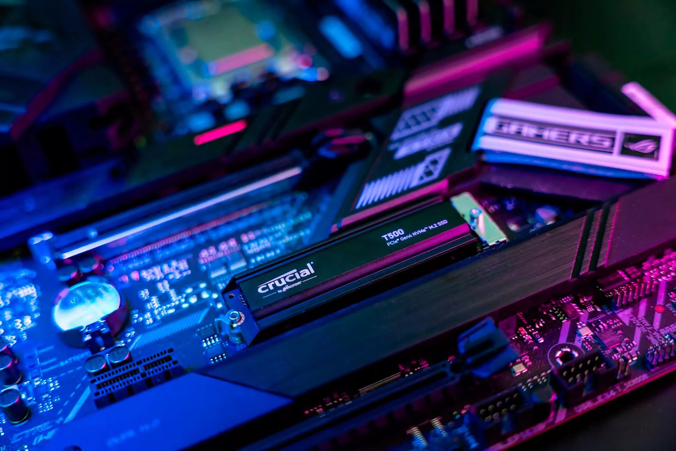
Freezing edge expertise: A brand new plasma-based etching course of may result in denser information storage in telephones, cameras, and computer systems. Researchers have developed a hydrogen fluoride plasma approach that doubles the etching fee within the manufacturing means of 3D NAND flash reminiscence chips.
Normal NAND flash storage is utilized in microSD playing cards, USB drives, and solid-state drives in computer systems and telephones. To suit extra gigabytes into smaller areas, producers have begun stacking reminiscence cells vertically in a course of referred to as 3D NAND.
Developments in 3D NAND have pushed chip designs past 200 layers, with corporations like Micron, SK Hynix, and Samsung already eyeing 400-layer expertise to extend storage density. Nonetheless, larger layer counts additionally carry better manufacturing complexity. One significantly demanding course of is etching, which requires meticulously carving exact holes, layer by layer, via alternating silicon oxide and silicon nitride layers.
Researchers from Lam Analysis, the College of Colorado Boulder, and the Princeton Plasma Physics Laboratory (PPPL) have developed a brand new approach to streamline the method. It makes use of cryogenic (low-temperature) hydrogen fluoride plasma to etch the holes. In experiments, the etch fee greater than doubled, rising from 310 nanometers per minute with the outdated methodology to 640 nm/min with their method. In addition they discovered that the etched holes had been cleaner.

Seeing advantages, the researchers experimented with including just a few different elements to the hydrogen fluoride plasma recipe. Phosphorus trifluoride acted as a nitrous enhance for silicon dioxide etching, quadrupling the speed. In addition they examined ammonium fluorosilicate. The staff detailed its findings in a research printed within the Journal of Vacuum Science & Know-how.
Seeing advantages, the researchers explored including just a few different elements to this hydrogen fluoride plasma recipe. Phosphorus trifluoride acted as a nitrous enhance for the silicon dioxide etching, quadrupling that fee. In addition they examined out ammonium fluorosilicate. The complete findings could be discovered within the research printed within the Journal of Vacuum Science & Know-how.
Whereas some challenges stay, the brand new approach may overcome a major manufacturing hurdle. Igor Kaganovich, a principal analysis physicist at PPPL, identified that rising reminiscence density will likely be essential as information calls for develop with AI adoption.
It is too early to say if it will lead to cheaper or denser NAND chips for customers. The approach nonetheless must be confirmed commercially viable and scaled for mass manufacturing. Even when producers undertake the method, there is no assure that any value financial savings will trickle all the way down to customers.
Freezing edge expertise: A brand new plasma-based etching course of may result in denser information storage in telephones, cameras, and computer systems. Researchers have developed a hydrogen fluoride plasma approach that doubles the etching fee within the manufacturing means of 3D NAND flash reminiscence chips.
Normal NAND flash storage is utilized in microSD playing cards, USB drives, and solid-state drives in computer systems and telephones. To suit extra gigabytes into smaller areas, producers have begun stacking reminiscence cells vertically in a course of referred to as 3D NAND.
Developments in 3D NAND have pushed chip designs past 200 layers, with corporations like Micron, SK Hynix, and Samsung already eyeing 400-layer expertise to extend storage density. Nonetheless, larger layer counts additionally carry better manufacturing complexity. One significantly demanding course of is etching, which requires meticulously carving exact holes, layer by layer, via alternating silicon oxide and silicon nitride layers.
Researchers from Lam Analysis, the College of Colorado Boulder, and the Princeton Plasma Physics Laboratory (PPPL) have developed a brand new approach to streamline the method. It makes use of cryogenic (low-temperature) hydrogen fluoride plasma to etch the holes. In experiments, the etch fee greater than doubled, rising from 310 nanometers per minute with the outdated methodology to 640 nm/min with their method. In addition they discovered that the etched holes had been cleaner.
Seeing advantages, the researchers experimented with including just a few different elements to the hydrogen fluoride plasma recipe. Phosphorus trifluoride acted as a nitrous enhance for silicon dioxide etching, quadrupling the speed. In addition they examined ammonium fluorosilicate. The staff detailed its findings in a research printed within the Journal of Vacuum Science & Know-how.
Seeing advantages, the researchers explored including just a few different elements to this hydrogen fluoride plasma recipe. Phosphorus trifluoride acted as a nitrous enhance for the silicon dioxide etching, quadrupling that fee. In addition they examined out ammonium fluorosilicate. The complete findings could be discovered within the research printed within the Journal of Vacuum Science & Know-how.
Whereas some challenges stay, the brand new approach may overcome a major manufacturing hurdle. Igor Kaganovich, a principal analysis physicist at PPPL, identified that rising reminiscence density will likely be essential as information calls for develop with AI adoption.
It is too early to say if it will lead to cheaper or denser NAND chips for customers. The approach nonetheless must be confirmed commercially viable and scaled for mass manufacturing. Even when producers undertake the method, there is no assure that any value financial savings will trickle all the way down to customers.


